Years ago, back when every conference had an “IoT track” and nobody was talking about LLMs yet, I bought a Nandland Go Board with the intent of learning FPGAs. The board went into a drawer, life happened, and I never got around to it. A few project ideas have brought FPGAs back to the front of my mind, so I pulled the Go Board out of the drawer and went back to basics using an entirely open-source toolchain on Fedora.
This post is about that toolchain. The Nandland book and tutorials walk you through Lattice’s vendor tools, which work fine but aren’t open source and aren’t a great fit for a Linux workstation. The good news is that the iCE40 part on the Go Board is exactly the family that the open-source FPGA tools support best — and on Fedora 43, the whole stack is one dnf install away.
The Go Board
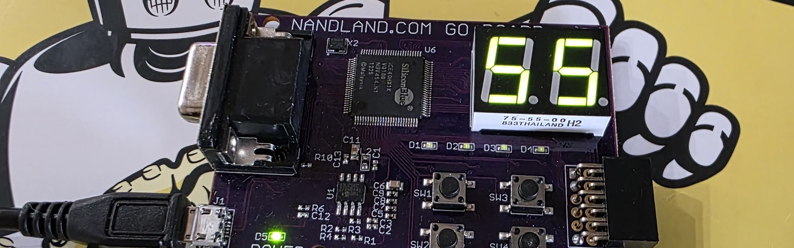
The Nandland Go Board is a small, beginner-oriented FPGA development board built around a Lattice iCE40 HX1K. On board you get four LEDs, four pushbuttons, a couple of seven-segment displays, a VGA connector, a UART-over-USB bridge, and a handful of PMOD-style headers. It’s dated by current standards — there are flashier boards out there now — but as a learning board it’s still a great pick. The peripherals are simple enough that you can light them up without drowning in IP cores, and there’s enough variety to keep early projects interesting.
A side benefit of the Go Board specifically: the iCE40 HX1K is the original target of Project IceStorm, the first fully open-source FPGA toolchain. So the board you’d buy to learn from a beginner book also happens to be the board the open-source ecosystem cut its teeth on. Lucky alignment.
The Book
I worked through Russell Merrick’s Getting Started with FPGAs, which is written by the same person behind Nandland and the Go Board. It’s a solid introduction — paced for someone who’s done some embedded or digital logic but is new to HDL, with exercises that you can run on the Go Board as you go. I went through the whole book and all of the exercises, and I’d recommend it as a starting point.
The one caveat is the toolchain. The book and the Nandland site both target Lattice’s iCEcube2 / Diamond / Radiant tools. Those work, but they’re closed-source vendor tools with the usual frustrations: license registration, a Windows-first install path, and an experience that feels disconnected from how I work on everything else. I went looking for an open-source path from the start.
The Open-Source Toolchain
The open-source iCE40 flow has three pieces, and they map cleanly to the stages of a traditional FPGA build:
| Stage | Tool | What it does |
|---|---|---|
| Synthesis | yosys | Compiles Verilog (or SystemVerilog) into a technology-mapped netlist for the target FPGA family. |
| Place & route | nextpnr | Takes the netlist plus constraints (pin assignments, clock targets) and figures out which logic goes where on the chip and how to wire it. |
| Bitstream + flashing | Project IceStorm | Packs the routed design into a .bin bitstream (icepack) and flashes it to the board (iceprog). |
All three are actively developed under the YosysHQ umbrella, all three are in Fedora’s repos, and all three Just Work for the iCE40 family. This is the same toolchain that big open hardware projects like TinyFPGA and a lot of community-built iCE40 boards rely on.
A few things that aren’t strictly part of the toolchain but pair nicely with it:
- Icarus Verilog (
iverilog) — a Verilog simulator. You’ll want this for testbenches, since simulating before you synthesize is the whole point of HDL. - GTKWave — viewer for the VCD waveforms that
iverilogproduces. Pretty much required for debugging anything past trivial issues.
Installing on Fedora 43
On Fedora 43, all of this is in the standard repos:
| |
That’s the whole install. No emailing a human to get a license file mailed back, no registration, no installer GUI to fight with. Compare that to the vendor flow and you can see why I switched.
To talk to the Go Board you’ll also want udev rules so iceprog can access the FT2232H USB bridge without root. Fedora’s icestorm package drops these in /usr/lib/udev/rules.d/ — they tag the device with uaccess, which grants access to whoever is logged in at the active console session, so no group membership is needed. If iceprog still complains about permissions, adding yourself to the dialout group is usually enough.
The Build Flow
Here’s the whole flow for a Go Board (iCE40 HX1K, VQ100 package) project, end to end. Assume you’ve got a Verilog source top.v and a pin constraints file top.pcf.
| |
Four commands. Each one does one thing, and you can inspect the output of each stage as a regular file — the JSON netlist, the ASCII placement, the final binary. That’s a different experience from the vendor tools, where the intermediate state is mostly opaque.
If your design spans multiple Verilog files (which it will, as soon as you’re past blinking an LED), just list them all on the yosys command line:
A Makefile glues this together nicely. Most of the open-source iCE40 example projects you’ll find on GitHub use roughly the same four-stage Makefile, often with make for build and make prog for flash.
What Yosys Is Doing (and What to Look For)
synth_ice40 isn’t a single operation — it’s a canned script that runs ~50 passes in sequence: parse the Verilog, elaborate the module hierarchy, run constant folding and dead-code elimination, identify finite state machines, infer block RAMs and DSP blocks, map generic logic onto the iCE40’s primitives (SB_LUT4, SB_DFF, SB_CARRY, SB_RAM40_4K), and finally emit the JSON netlist that nextpnr will consume. You can see all of this fly by in the console — it’s a lot of output, and most of it you can ignore. Yosys is loud by default, but only a few things in that output actually matter.
The resource utilization summary at the end. Yosys prints a stats block right before the JSON backend runs. For one of the Nandland website exercises (a UART receiver feeding two 7-segment displays):
This is the part of the output to actually pay attention to. SB_LUT4 counts 4-input lookup tables, SB_DFF* counts flip-flops, and SB_CARRY counts carry cells. The HX1K has 1280 LUTs total, so 81 LUTs is a tiny fraction of the chip — plenty of room. As designs get bigger, this is the first place to look to see how close you are to running out of fabric. If you blow past 100% you’ll find out at place-and-route, but you’d rather know here.
Warnings. A clean run, like the one above, ends with Found and reported 0 problems from the final CHECK pass. Anything earlier flagged as Warning: deserves a look — common ones are inferred latches (almost always a bug — usually a missing else in a combinational always block), multi-driven nets, and width mismatches. Yosys will happily synthesize a design with warnings, but those warnings are usually the difference between code that works and code that almost works. Pipe the output through grep when you need to find them quickly:
| |
The CPU and memory line at the very bottom. Yosys prints its total CPU time and peak memory use on the last line of the run. If that line is there, the run finished cleanly — useful when you’re skimming a long log and want to confirm it didn’t get truncated. The UART/7-seg example above takes a fraction of a second on a modern laptop, and even designs in the thousands of LUTs still finish in seconds.
Everything else — the per-pass debug output, the optimizer’s running tallies of cells removed, the ABC9 mapping output, the Generating RTLIL representation lines — is internal bookkeeping. Skim it when you’re curious, ignore it when you’re not.
A practical habit: redirect the output to a log file so the terminal stays readable but the full record is there if you need to dig in later.
| |
Constraints
nextpnr needs two pieces of design context that aren’t in the Verilog: pin assignments (which top-level signal goes to which physical FPGA pin) and clock targets (what frequency the timing analyzer should treat each clock as running at). The open-source flow uses two text formats for these — .pcf for pin assignments and .sdc for clock constraints.
Conveniently, the Nandland book and site already publish a Go_Board_Constraints.pcf and a Go_Board_Clock_Constraint.sdc in exactly those formats. They can be passed straight to nextpnr, no translation needed. The PCF defines every pin on the Go Board (LEDs, buttons, seven-segments, VGA, PMOD headers, the UART pins), so you can reuse it across every project on the board. nextpnr will warn about constraints that don’t match any signal in your top module, which is fine and expected when a project only uses a subset of the pins — more on that in the next section.
What nextpnr Is Doing (and What to Look For)
nextpnr-ice40 does three things in sequence: pack the netlist’s logic primitives into the iCE40’s physical cells (LUTs and FFs into LCs, carries into carry chains, etc.), place each cell onto a specific location on the chip, and route the wires between them. Then it runs static timing analysis on the routed design and tells you whether it will actually meet the clock frequency from the SDC.
The full invocation pulls in both the PCF and the SDC via --pcf and --sdc:
The Go Board’s SDC is a single line that tells nextpnr to treat i_Clk as a 25 MHz clock (40 ns period). Without an SDC, nextpnr still reports a max frequency, but there’s no PASS/FAIL because there’s no target. With it, you get a clear pass/fail at the bottom of the run.
Like yosys, nextpnr is loud. The four things actually worth reading:
Pin constraint resolution. Near the top of the run you’ll see a line per IO that nextpnr matched to a physical pin (Info: constrained 'o_Segment1_A' to bel 'X0/Y13/io1') and a warning per constraint that didn’t match anything in the design (Warning: unmatched constraint 'o_LED_1'). The unmatched warnings are normal when you use a board-wide PCF for a project that only touches a subset of the pins — nextpnr is just letting you know it ignored those lines. They’re worth a glance to make sure you didn’t typo a port name (a typo’d output port silently becomes a warning, not an error).
Device utilization. After packing, nextpnr prints the post-pack resource block:
This is the more honest version of yosys’ submodule count. yosys reports cells before packing — separate LUTs and FFs. nextpnr reports them after packing, where LUT+FF pairs share a single logic cell (LC). The 81 LUTs + 35 FFs that yosys reported above pack down to 89 LCs here, which is what actually fits on the chip. SB_IO is your I/O pin count, SB_GB is global buffers (clock distribution), and ICESTORM_RAM / ICESTORM_PLL count block RAMs and PLLs. If you’re getting close to 100% on any line, you’re getting close to needing a bigger part.
The max frequency PASS/FAIL. This is the headline result. You’ll see it twice — once after initial placement, once after routing — and the post-routing one is the real number:
| |
PASS at 25.00 MHz means the design will run at the clock you constrained. The 188 MHz is the maximum frequency the routed design could run at — i.e., your timing margin. For a 25 MHz design that’s enormous headroom; for designs pushing the chip you’ll see this number drop toward your target, and once it goes under, it’s FAIL.
If you do hit FAIL, the critical path report below the frequency line tells you exactly which signal path is too slow — every cell and wire on the worst path, with cumulative delay in nanoseconds. That’s where you start looking when timing doesn’t close.
The final summary line. 28 warnings, 0 errors followed by Program finished normally. — errors here mean the design didn’t make it to a bitstream. Warnings, as above, are usually fine but worth a scan.
Packing and Flashing
After yosys and nextpnr, the last two steps are the easy ones.
icepack converts the ASCII bitstream nextpnr produced into the binary bitstream the iCE40 actually accepts. It’s silent on success:
| |
No output, just a fresh .bin file. If icepack says anything, something’s wrong.
iceprog flashes that binary to the SPI flash on the Go Board over USB (via the on-board FT2232H bridge — the same chip that provides the UART-over-USB interface). The output is short and worth reading every time:
Three things to glance at:
flash ID:— confirmsiceprogactually talked to the SPI flash. If you see all0xffor all0x00here, it didn’t. Usually a permissions issue (see below) or the board isn’t powered.VERIFY OK—iceprogreads back what it wrote and compares. If verify fails, the bitstream on the chip doesn’t match the file.cdone: high(the second one) —cdoneis the iCE40’s “configuration complete” pin. After flashing, the FPGA reloads from SPI flash and assertscdoneonce it’s running. High at the end means your design is alive on the board.
If you get Can't find iCE FTDI USB device or a permission error, it’s usually udev. The icestorm package on Fedora drops in a rules file that grants access via uaccess to the active console user, so the most common fix is to make sure you’re running iceprog from a graphical login session rather than a remote SSH session. As a quick sanity check, lsusb should show an FTDI device when the Go Board is plugged in.
Simulating With Icarus Verilog and GTKWave
Synthesis tells you whether a design fits and meets timing; it doesn’t tell you whether it’s actually correct. For that you simulate.
The Nandland book and site recommend EDA Playground for this — a browser-based environment that’s free to use and works fine. But it’s a hosted service, and one of the points of switching toolchains was to keep everything local. The open-source side has a complete answer here too: Icarus Verilog compiles your Verilog (and SystemVerilog testbenches) into a runnable simulator, and GTKWave shows you the resulting waveforms. Both are in Fedora’s repos (already in the dnf install line above), and the whole loop runs offline.
The flow is three commands. Compile the design and testbench, run the simulation, then open the dumped waveforms:
Icarus Verilog ships with two binaries: iverilog (the compiler) and vvp (the runtime that executes the compiled simulation). gtkwave is a separate package for the viewer. The -g2012 flag tells iverilog to accept SystemVerilog 2012 syntax — Nandland’s testbenches are .sv files, so this matters. Without it, anything past basic Verilog-2005 will fail to parse.
The vvp output is short and worth reading:
The VCD info line confirms the waveform dump file was created. The VCD warning here is harmless — it just means iverilog can’t dump package-scope items into VCD format, which doesn’t affect the actual signal traces. The Test Passed line is from the testbench itself — Nandland’s testbenches print a pass/fail message via $display, which is a clean pattern worth borrowing in your own. And $finish called tells you the simulation ran to completion rather than getting stuck.
gtkwave dump.vcd opens the viewer. You select the signals to display in the left pane, and the wave window shows exactly what each register and wire was doing on each clock edge. Here’s the UART_RX project mid-simulation, receiving the byte 0x37:
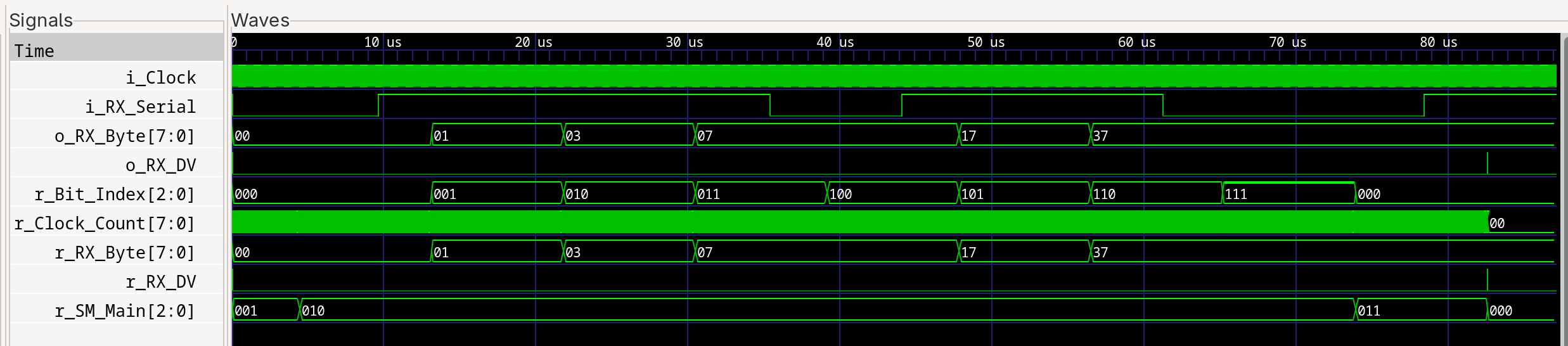
You can see the internal state machine r_SM_Main stepping through states, r_Bit_Index counting from 000 up to 111 as each bit is sampled, and r_RX_Byte building up the received value (00 → 01 → 03 → 07 → 17 → 37) one bit at a time. That’s the kind of visibility that makes hardware debugging tractable.
A couple of GTKWave usability notes that aren’t obvious the first time you open it:
- The wave view starts empty. When you open a VCD, you have to populate the wave window yourself — pick a module from the upper-left pane, select the signals you care about from the lower-left list, and click Append (or Insert) to drop them into the wave window. Until you do, the view on the right is blank.
- It opens zoomed way in. Default zoom shows a tiny slice of time — often microseconds out of a milliseconds-long simulation — so it looks like nothing is happening. Use the zoom controls (or View → Zoom Fit) to get a useful overview, then zoom in on the interesting region.
- Save your layout. Once you’ve got your most-watched signals in the wave window, File → Write Save File dumps a
.gtkwsave file. Re-open withgtkwave -a saved.gtkw dump.vcdto skip the signal-picking step next time.
GTKWave is showing its age in the UI department — the toolbar buttons look like a 2003 GTK app, because they basically are — but it’s solid software once you’ve got the muscle memory for it.
Working Through the Nandland Exercises
I haven’t written any Verilog in this post on purpose — Nandland’s tutorials and the book already cover that ground better than I would, with a curriculum that builds from blinking LEDs up through UARTs and VGA. If you’re using this post to get started, work through their material for the HDL side and substitute the four-command toolchain above for the iCEcube2 build steps they walk through. The Verilog is identical; only the build flow changes.
The example I’ve been using throughout this post — the one whose synthesis, place-and-route, and simulation output you’ve seen excerpts of — is Nandland’s UART Receiver tutorial wired up to the Go Board’s two seven-segment displays. It’s a good intermediate exercise: a state machine, a few sub-modules, an actual external interface to test against, and small enough that the whole build runs in well under a second. If you want to follow along with exactly the artifacts this post showed, that’s the project to start with.
Resources
- Nandland Go Board
- Getting Started with FPGAs — Russell Merrick
- yosys · nextpnr · Project IceStorm
- Icarus Verilog · GTKWave
- Lattice iCE40 family page (datasheets and pinouts)